During my architecture of computers course, I decided I wanted to go a little bit deeper than the course did on how a CPU works. Obviously, this meant i needed to build my own, gate-by-gate.
I started out by picking a simulator to build a CPU with (because the real world sucks), and eventually settled on Virtual Circuit Board: it’s a great simulator, and it looks nice too. Then, I went ahead and built some basic circuitry that I knew I’d need, like an 8-bit adder and registers. This all was fairly straightforward– the adder, well, added numbers. It wasn’t too complicated. However, I still had no idea where to start the CPU itself.
So, without any clue as to how to structure the CPU, I was lost. So, I googled. And googled. You know, the internet has everything these days. However, most of the documents I found online were either too complicated for me to understand when I’d never built a CPU at all before, or it didn’t really have enough detail to be useful. Not many fell in the middle. I ended up consulting someone I knew that understood this stuff and they told me that I should begin by making an instruction set architecture, and then a finite state machine for the control circuitry.
I knew that I wanted my CPU to be simple, so I stuck with 8-bit data and 16-bit addresses. I don’t remember much else (this blog is a recap of everything that’s happened), but the overall instruction set ended up looking like this:
| Instruction | Description |
|---|---|
| ASTL | Set accumulator low to constant |
| ASTH | Set accumulator high to constant |
| MSTL | Set memory pointer low to accumulator |
| MSTH | Set memory pointer high to accumulator |
| OPER | Perform ALU operation given by constant Accumulator is input A and temp register is input B Output to accumulator |
| JUMP | Offset program counter by accumulator - 0x7F |
| JMPZ | Offset program counter by accumulator - 0x7F if status register signals 0 |
| JMPO | Offset program counter by accumulator - 0x7F if status register signals overflow |
| LOAD | Load the contents of memory location X into the accumulator, where X is the contents of the memory pointer + constant |
| STOR | Store the contents of the accumulator into memory location X, where X is the contents of the memory pointer + constant |
| SWAP | Swap the contents of temporary register and the accumulator |
| MADD | Add the accumulator to the memory pointer |
There are two 8-bit registers and one 16-bit register accessible to the programmer, respectively the accumulator, temporary register, and memory pointer.
The accumulator serves as one of two operands for the OPER instruction, with the temp register being the other.
The memory pointer is used as a base address register for memory operations, such as LOAD and STOR
Each instruction uses the upper 4 bits to determine what to do, and the lower 4 bits are constant data.
The purpose of the finite state machine for the control circuitry is to determine which control lines should be active at any time. Each state has an output bit for each control line and rules to determine which state to transition to on the next clock cycle.
Given the general CPU order of operations, I knew the states had to go something like
fetch instruction > increment program counter > execute instruction.
Fetching the instruction was fairly simple and consisted of three states, aptly A, B and C. State A told the program counter to output to the address bus, and that the memory address in should read from the address bus. State B sets the memory to output to the data bus. State C keeps outputting the memory to the data bus, but also tells the instruction register to read from the data bus. Incrementing the program counter was pretty similar.
The transition logic looks like this: A > B > C > INCPC A > INCPC B > ??, where ?? are the instruction-specific states. Now, since these states vary based on what the instruction register is, the instruction register is an input to the state machine. Most of the time, it doesn’t care about the instruction register. The one exception is when the current state is INCPC B. This is the state right before the instruction starts to execute.
After an instruction is selected, the state machine goes through each state required to run the instruction. For example, the ASTH instruction has two states ASTH A and ASTH B.
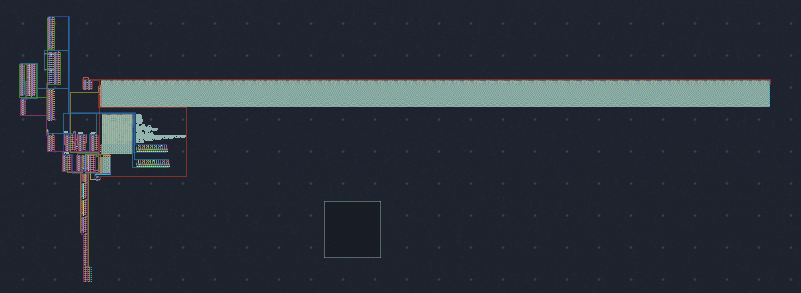
With the finite state machine complete, I then had to get it into the simulator. Of course, I wasn’t going to place every gate by hand for the state transition lookup table, so I found a program to do it for me: vcbtool. However, the lookup table generator in this application doesn’t allow “don’t care” bits, so I wrote a short program to convert the truth table to not use “don’t care” bits. This lazy workaround cost a lot of space in the simulator, though, since every possible combination of “don’t care” bits needed to be explicitly set as 0 or 1 in the lookup table.
For reference, here’s a screenshot of the entire CPU. The long strip of gates is the transition lookup table.

Generating the state machine output was easier since there were no “don’t care” bits in the output, and any invalid states would output 0 if not in the lookup table.
All that was left was to wire together the components I made at the very beginning with the control circuitry. At least, I thought. The timing was off for some instructions, and they didn’t work properly as a result. This took a while to debug as I had to step through the simulation and watch the individual gates flip to figure out how to adjust the timing.
You can get the latest version of the design here.